
key features of your Pcb production and assembly
Printed Circuit Board (PCB) production and assembly are intricate processes that form the backbone of modern electronic devices. From consumer electronics to industrial machinery, PCBs are essential for creating reliable and efficient electronic circuits. The key features of PCB production and assembly encompass a wide range of considerations, from design and material selection to manufacturing processes and quality control. Understanding these features is crucial for ensuring the performance and longevity of the final product.
One of the primary features of PCB production is the design phase. This phase involves creating a detailed layout of the circuit, which includes the placement of components and the routing of electrical connections. Advanced software tools are used to design PCBs, allowing for precise control over the layout and ensuring that the board can accommodate the required components. Design considerations also include signal integrity, thermal management, and manufacturability, all of which are critical for the PCB’s performance and reliability.
Material selection is another vital aspect of pcb production and assembly. The choice of materials affects the board’s electrical properties, thermal performance, and durability. Common materials include FR-4, a fiberglass-reinforced epoxy laminate, which offers a good balance of performance and cost. For high-frequency or high-temperature applications, materials such as polyimide or ceramic substrates may be used. The selection of copper cladding thickness is also important, as it influences the current-carrying capacity and thermal management of the PCB.
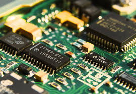
What are the key features of your Pcb production and assembly?
The manufacturing process of PCBs involves several steps, including etching, drilling, and plating. Etching removes unwanted copper from the board to create the desired circuit pattern. Precision in this step is crucial to ensure that the circuits are correctly formed without defects. Drilling creates holes for component leads and vias, which connect different layers of the PCB. These holes must be accurately positioned and sized to fit the components and ensure reliable electrical connections. Plating involves depositing a thin layer of metal, typically copper, onto the drilled holes and circuit traces, enhancing conductivity and durability.
Solder mask application and silkscreen printing are additional manufacturing steps that enhance the functionality and appearance of the PCB. The solder mask is a protective layer that prevents solder bridges between closely spaced components and protects the board from environmental damage. Silkscreen printing adds labels and symbols to the PCB, aiding in component placement and providing important information for assembly and troubleshooting.
PCB assembly involves placing and soldering components onto the board. This process can be performed using surface mount technology (SMT) or through-hole technology (THT), depending on the type of components and the design of the PCB. SMT is commonly used for small, lightweight components and allows for higher component density, while THT provides stronger mechanical bonds, making it suitable for larger or heavier components. Automated assembly machines ensure precision and consistency in component placement and soldering, which are essential for the functionality of the final product.
Quality control is a critical feature of PCB production and assembly. Rigorous testing procedures, such as automated optical inspection (AOI), X-ray inspection, and in-circuit testing (ICT), are employed to detect defects and ensure that the PCBs meet the required specifications. These tests check for issues such as solder joint integrity, component orientation, and electrical connectivity, helping to identify and correct problems before the boards are shipped to customers.
In conclusion, the key features of PCB production and assembly encompass a comprehensive approach to design, material selection, manufacturing processes, and quality control. Each step plays a crucial role in ensuring that the final product meets the desired performance and reliability standards. By understanding and optimizing these features, manufacturers can produce high-quality PCBs that form the foundation of modern electronic devices.


