
Software Used in HDI PCB Design
Using smaller components, compacted routing and buried vias, HDI PCBs allow you to fit more circuitry into a much smaller package. This provides advantages like better signal integrity, lower power consumption and faster time to market. These advantages can be found in medical, cell phone and IoT devices as well as many other applications. But to design an effective HDI board requires advanced tools and software that have been developed specifically to work with the unique manufacturing process of HDI.
These include new and unique materials, laser drilling, sequential build up and more. On the design side, the PCB design software needs to accommodate the increased precision needed in tighter trace widths and spacing, a greater range of via types including microvias, and the ability to handle the complex stack ups that are typical with HDI boards.
Among the most important tools for a PCB designer are the CAD (computer-aided design) tools used to create the schematics and the layout of the board. These CAD tools help to make sure that all the components and connections are in place, that the proper layer separations have been established, and that the board will be easy to produce by the manufacturer. In addition, these CAD tools also provide the foundation for the Gerber files that are used to represent the data to be transferred to the manufacturer for fabrication of the board.
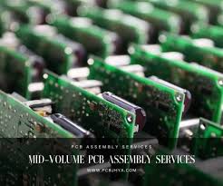
Tools and Software Used in HDI PCB Design
When it comes to the specialized tools that are used for HDI PCB design, there are several of them that are commonly utilized. These include the use of microvias, which are small via structures that are drilled in a manner that allows them to be filled with copper. These are often used to connect inner layers of the board. In some cases, the inner layers of an hdi board are connected through a series of staggered or skip microvias with buried vias connecting between these.
Another essential tool for the HDI design process is the ability to accurately predict and design the impedance of each trace and layer. This is accomplished by using advanced simulation technology and solvers that can be accessed directly from the PCB layout environment. These include the Cadence Sigrity and Celsius solvers that can check impedance, crosstalk, return path, power loss and more. In addition, these Sigrity and Celsius tools can easily be integrated into the Altium Designer PCB layout environment.
The choice of the components for a HDI board is also important. This can influence the choice of routing widths, location and type of drilled holes and vias in the stack-up and also the overall manufacturing cost of the finished product.
Altium is the premier PCB design software platform that offers these specialized tools to help designers with their HDI board designs. With features like schematic, ECAD libraries, rules and constraints, Bill of Material (BoM), supply chain management, ECO processes and world-class PCB layout tools, the platform makes it easy to work with any HDI project.


