
PCB Fabrication Assembly
Rigorous quality control measures must be put in place to ensure that PCBs can be fabricated and assembled correctly. Failure to do so can lead to a host of problems in the final product such as poor functionality, cost overruns, and reduced brand reputation. These defects can be attributed to a variety of issues including improper manufacturing processes, design oversights, or other factors such as material shortages or component availability. This makes it crucial for designers to take the time to understand the limitations of pcb fabrication assembly and address any potential problem areas during the layout phase.
Designing for Manufacture (DFM) guidelines can help avoid many of these issues. Following these rules will allow you to make the most of the capabilities of your contract manufacturer (CM) and speed up production. It is also a good idea to run a pilot production run to check for any issues that need to be addressed before going into full-scale production.
Insufficient clearances or inaccurate measurements are among the most common causes of faulty pcb fabrication assembly. This can result in solder connections that are not secure or a lack of continuity across layers. Plating defects such as nodules (bumps on the plated copper surface), pits, dull textured coating, thinner plating than the required specifications, and pin holes that are too small for their respective parts can also cause connectivity problems.
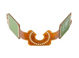
Limitations of PCB Fabrication Assembly
Another problem that can arise is the use of unsuitable materials or improper soldering techniques. In some cases, these defects can be difficult to trace back to their source and may require extensive testing to identify. This can be a major headache that can cost time and money, especially if the defective board is used for critical applications such as military or aerospace systems.
Some of these defects can be avoided by ensuring that the correct thickness of the base layers is utilized and that the proper etching solution is used. It is also advisable to ensure that the components that generate heat are placed in an area with sufficient air circulation or near a heat sink to prevent overheating. In addition, the correct soldering techniques must be employed to prevent overheating of the solder joints and other damage.
The integration of Industry 4.0 principles has also revolutionized PCB assembly. Smart factories equipped with IoT-enabled devices and advanced analytics allow manufacturers to monitor and optimize every aspect of production in real-time. Data from sensors and machines can be used to predict maintenance needs, reduce downtime, and improve overall efficiency.
Providing detailed documentation is also vital for a smooth PCB manufacturing process. Clearly labeling critical dimensions and documenting any special requirements will make it easier for the CM to troubleshoot any errors that might occur during the process. It is also a good idea to consider test design when laying out the circuit board and incorporate access points for in-circuit and functional testing. This will save valuable time and money by reducing the need for expensive rework, redesigns, and other quality control activities.


