
assembly considerations for HDI PCBs
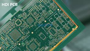
The high-density interconnect PCB (HDI) is a type of printed circuit board used in the design of electronic devices and systems. These PCBs are smaller and more dense than traditional PCBs, allowing for more components to be fitted into a single board.
The assembly process for HDI PCBs requires more consideration than standard printed circuit boards, as the size and density of the parts can increase the likelihood of errors or failure. This is why it is crucial to consider the assembly considerations for hdi pcb at an early stage of the design process. Incorporating Design for Assembly (DfA) principles into the process can help ensure that the board meets its intended functionality, minimizes risk, and prevents costly revisions during production.
Assembling an hdi pcb requires precise placement of components. This is because the spacing between traces on an HDI PCB is very tight, meaning that any errors made during assembly could lead to problems with the function of the device. Using DfA principles at an early stage of the design process can help avoid these mistakes.
What are the assembly considerations for HDI PCBs?
One of the most important assembly considerations for a HDI PCB is the selection of materials. This is because the material choice can have a big impact on the electrical performance of signal traces. For example, copper is typically used for signal traces, and it must be treated with an organic solderability preservative to maintain good conductivity. It is also common to use polyimide materials such as DuPont Pyralux AP and Panasonic Felios for rigid-flex circuit boards, which offer excellent thermal stability and low Z-axis expansion.
Another key assembly consideration for HDI PCBs is the use of microvias to replace through-hole vias. This is because it allows the designer to reduce the amount of copper on the PCB while maintaining adequate signal integrity and power delivery capability. In order to fabricate these microvias, the fabricator must etch holes that are smaller than the standard through-holes in the PCB. They also must be placed in the correct layers of the PCB. For example, it is not acceptable to place blind or buried microvias in layers that contain traces or components, as this violates the DFM rules of many manufacturers and will cause them to reject the PCB.
As a result, it is vital to pay attention to the details of the fabrication process for an HDI PCB in order to ensure that it complies with all IPC standards. This can be done by ensuring that the design team has taken all the relevant manufacturing constraints into account. The best way to do this is to use a PCB modeling software program. This will allow the design team to visualize and understand how their layout will perform during the fabrication process and identify any issues that may arise. This will help them to resolve any problems and reduce the time needed for assembly. This will also help to improve the overall quality of the finished product.


