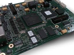
signal integrity in pcb circuit board assembly
In the realm of electronics, maintaining signal integrity is paramount for the reliable operation of electronic devices. Signal integrity refers to the preservation of signal quality as it travels through a Printed Circuit Board (PCB) and its associated components. Any degradation or distortion of signals can lead to communication errors, reduced performance, or even device failure. PCB circuit board assembly plays a critical role in ensuring signal integrity by employing various techniques and best practices throughout the design, fabrication, and assembly process.
One of the primary considerations for ensuring signal integrity in pcb circuit board assembly is proper layout and routing of signal traces. High-speed signals, such as those used in high-speed data transmission or RF communication, are particularly susceptible to interference, crosstalk, and impedance mismatches. By carefully planning the layout of signal traces, avoiding sharp corners, minimizing trace lengths, and maintaining consistent trace widths, designers can minimize signal degradation and ensure impedance matching throughout the PCB.
Furthermore, the use of controlled impedance traces helps maintain signal integrity by matching the impedance of the transmission line to the impedance of the connected devices. By ensuring a consistent impedance profile along the signal path, controlled impedance traces reduce signal reflections and distortion, allowing for reliable transmission of high-speed signals with minimal loss. This is especially critical in applications where signal integrity is paramount, such as high-speed data communication or high-frequency RF systems.

How do you ensure signal integrity in pcb circuit board assembly?
In addition to layout considerations, proper grounding techniques are essential for ensuring signal integrity in PCB assembly. Ground planes provide a low-impedance return path for signals and help reduce electromagnetic interference (EMI) and noise coupling. By ensuring a solid ground plane and minimizing ground loops, designers can mitigate common sources of signal degradation and interference, ensuring cleaner signal transmission and reception.
Moreover, attention to component placement and decoupling capacitor placement is crucial for maintaining signal integrity. Placing critical components, such as microcontrollers or high-speed interface chips, close to their respective signal sources or destinations reduces trace lengths and minimizes signal skew. Decoupling capacitors placed strategically across the PCB provide a local energy reservoir, filtering out high-frequency noise and ensuring stable power delivery to sensitive components, further enhancing signal integrity.
The choice of PCB materials and fabrication techniques also impacts signal integrity in PCB assembly. High-quality substrate materials with low dielectric constant and low loss tangent minimize signal attenuation and dispersion, preserving signal integrity over longer distances. Additionally, advanced fabrication processes, such as controlled impedance manufacturing and multilayer PCB construction, ensure consistent electrical properties and impedance matching across the entire PCB, further enhancing signal integrity.
During the assembly process, attention to soldering techniques and material selection is essential for preserving signal integrity. Proper solder joint formation, including adequate solder fillets and minimal solder voids, ensures reliable electrical connections and minimizes signal loss. Additionally, the use of low-residue fluxes and solder mask materials helps prevent contamination and reduce the risk of signal degradation due to solder flux residues.
In conclusion, ensuring signal integrity in PCB circuit board assembly requires a comprehensive approach encompassing design, fabrication, and assembly considerations. By employing proper layout and routing techniques, controlling impedance, optimizing grounding, and selecting high-quality materials and fabrication processes, designers and manufacturers can minimize signal degradation and ensure reliable operation of electronic devices. As the demand for high-speed and high-frequency applications continues to grow, the importance of signal integrity in PCB assembly will only continue to increase, driving innovation and advancement in electronic design and manufacturing.


